

Monk9 Tech: A Ground-Up Vision for India’s Semiconductor Future
Monk9 Tech is building India’s first commercially accessible chip fab, aiming to democratize semiconductor manufacturing for start-ups, MSMEs, and academia.

Key Takeaways
- Monk9 Tech is pioneering India’s first legacy-node semiconductor fabrication facility.
- The startup offers affordable access to 350nm manufacturing for start-ups, MSMEs, and academic institutions.
- With a focus on open-source toolchains and design-to-tapeout support, Monk9 is enabling India’s chip self-reliance.
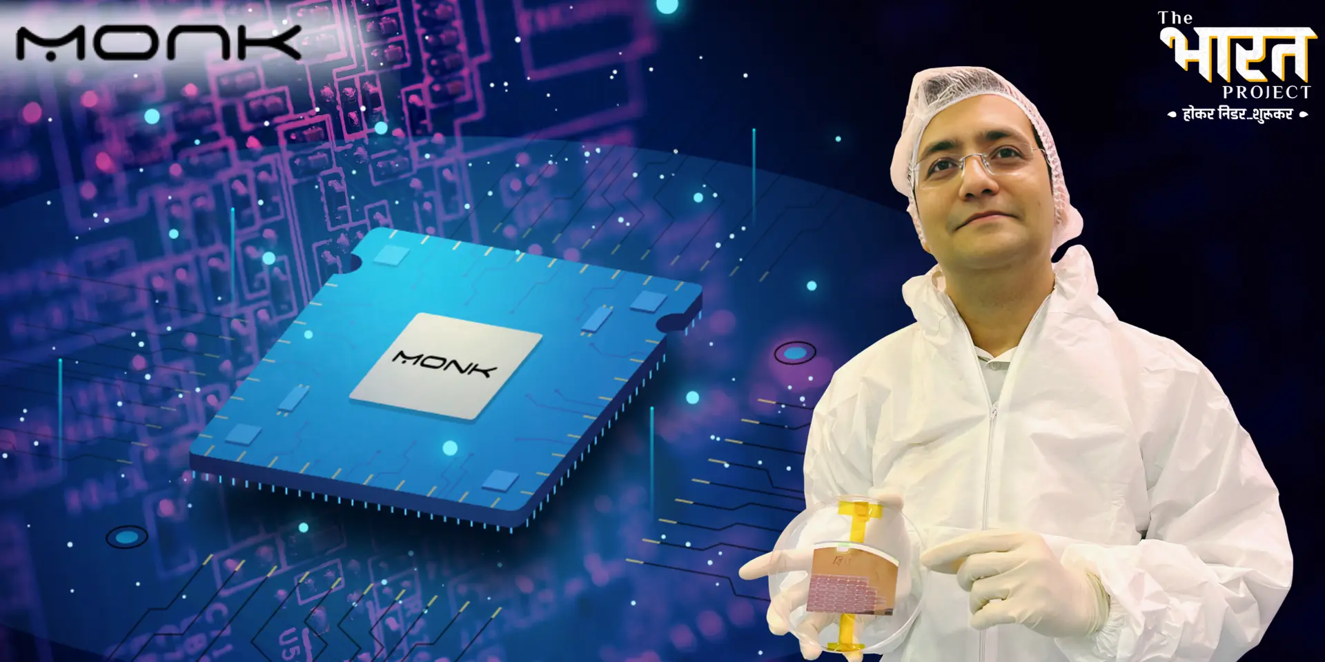
In 2022, amid global supply chain disruptions and rising geopolitical emphasis on tech sovereignty, Monk9 Tech Private Limited was born in Rajkot, Gujarat, with a bold ambition: to make chip manufacturing accessible to Indian innovators.
Founder Marmik Bhatt, who had previously worked across chip design and automation, saw a clear gap—India lacked affordable, indigenous semiconductor infrastructure, especially for legacy nodes.
Bridging India’s Fabrication Deficit
While chip design capabilities have grown in India, fabrication—particularly for legacy nodes like 350nm and 180nm—remains an import-dependent bottleneck. Monk9 aims to close this gap with India’s first open-access fab focused on 6-inch wafers at 350nm.

These nodes remain highly relevant for applications in IoT, automotive, defence, and industrial automation.
“The name ‘Monk9’ reflects our philosophy,” explains Bhatt. “‘Monk’ stands for deep thinking, and ‘9’ signifies technological evolution and power.”
Designed for Builders: Startups, MSMEs, Academia
Monk9’s user base spans early-stage product startups, Tier 2/3 engineering colleges, MSMEs, and R&D labs. These are precisely the groups that have historically struggled to access silicon tapeouts due to high costs, overseas lead times, and a lack of design support.
By offering tiered pricing, subsidised for academic users and market-aligned for industry, Monk9 makes legacy silicon accessible to a wider innovation base.
An Open-Source, India-First Model
Unlike large commercial foundries, Monk9 embraces open-source infrastructure. The startup has built RTL-to-GDS flows using tools from the Efabless OpenLane community and PDKs like Sky130. This approach reduces barriers to entry and promotes transparency in design.

“Open-source gave us the springboard we needed,” Bhatt notes. “From early prototypes to validated IP blocks, it’s allowed us to iterate quickly and educate users along the way.”
Market Potential and Revenue Streams
India’s demand for legacy chips—especially in IoT and automation—is estimated at over Rs 15,000 crore. Monk9 targets this segment with services that include foundry access, tape-out packages, chip prototyping, IP licensing, and design training. Its go-to-market strategy includes academic partnerships, design workshops, and collaboration with government innovation schemes.
Backed by Ecosystem Builders
Monk9’s journey has been supported by institutions like FITT-IIT Delhi, IIMA Ventures, and RK University. Government support under Gujarat’s Electronics Policy has helped align the startup’s vision with national manufacturing goals. The company also collaborates with global open-hardware networks like Efabless Corporation in Palo Alto.

Building from the Ground Up
The startup has already achieved key milestones: signing MoUs with universities, validating IP cores such as UART, ALU, and VGA sensors, and completing cleanroom and pilot fab layout plans. Monk9’s near-term focus is to operationalise its 350nm line, onboard the first 20 design customers, and release PDK V1.0.
Challenges and Learning Curves
The path hasn’t been easy. From sourcing refurbished equipment to building a fab-capable team, the challenges have been deeply technical and operational. But Bhatt remains grounded: “Start lean, iterate fast, and keep your mission rooted in real needs. That’s what sustains us.”
A Long-Term Vision for Full-Stack Capability
Beyond 350nm, Monk9 aims to expand into 180nm and 130nm nodes, introduce packaging and testing services, and evolve into a full-stack semiconductor manufacturing ecosystem. The long-term goal is clear: make India not only a design hub but a fabrication powerhouse.