



Ashwini Vaishnaw lays out six pillars of Semicon 2.0, from chip design to clean room talent
Union Minister Ashwini Vaishnaw outlined the six pillars of Semicon 2.0 at Semicon India 2026, spanning design, materials, fabs, packaging, applied R&D and talent.

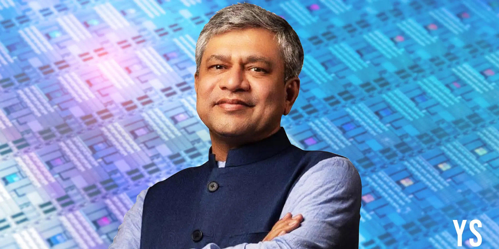

Union Minister for Electronics and Information Technology Ashwini Vaishnaw on September 17, 2026 set out the six pillars that will define Semicon 2.0, the second phase of India's semiconductor programme, at the inaugural session of Semicon India 2026 at Yashobhoomi in New Delhi.
Speaking ahead of Prime Minister Narendra Modi's address, he described the first phase as a "measured and calibrated" effort to get the industry to set up base in the country, and said the next round would build the industry over that foundation.
A foundation laid in five years
The India Semiconductor Mission was set up about five years ago, and 12 projects have been approved under the first phase. Five plants are now in commercial production after Suchi Semicon in Surat and CDIL in Mohali joined Micron, Kaynes and CG Semi at the same event.
The Prime Minister said the first phase was sized at about $8 billion, while the second has been set at up to $13.5 billion. Vaishnaw noted that more than 28 countries were participating in this year's conference, a sign of how far the supplier base has widened.
The six pillars of Semicon 2.0
Design is the first pillar. More than 105 startups took part in the design programme under the first phase, and about 20 of them raised roughly Rs 800 crore in venture funding. The new target is at least 200 startups and companies designing chips in India across the full range of semiconductor needs.
Machines and materials form the second pillar, covering capital equipment, maintenance services, chemicals and gases. Vaishnaw thanked Applied Materials for its $5 billion commitment announced at the same session, saying it would go a long way in generating employment.
The third pillar is more fabs, spanning display, memory, silicon, compound and logic. "The more the merrier," he said, arguing that the ecosystem builds over fabs and delivers a multiplier effect. Advanced packaging is the fourth pillar, with a 3D packaging unit already coming up in Odisha and more units sought.
Research and development is the fifth pillar, and here the minister was specific: the projects will be applied, industry-required work run jointly by industry and academia, not isolated research. He invited industry participants to suggest the projects they want taken up.
Talent is the sixth. The first phase promised 85,000 design engineers over 10 years; 70,000 have been trained in four. More than 400 universities now have EDA tools from Cadence, Siemens and Synopsys, and student designs are being taped out at the Semiconductor Laboratory in Mohali. Semicon 2.0 adds a target of one lakh technicians for clean rooms and factory floors.
Why does Semicon 2.0 talk about the ecosystem rather than fabs
Vaishnaw recalled the Prime Minister's early guidance: "Don't think fab, think ecosystem." A fab is the plant where wafers are processed into chips. It cannot run without equipment makers, gas and chemical suppliers, maintenance firms, packaging units and a steady pipeline of trained people.
Countries that dominate chipmaking built these surrounding layers over decades. Semicon 2.0 is designed to pull them into India at the same time as the fabs, so that each new plant has local suppliers and workers rather than importing everything.
What comes next
Vaishnaw called this the second step of a long journey towards Viksit Bharat. The immediate tests are how quickly the applied R&D projects get defined with industry, and whether the technician programme can produce clean room-ready workers as the 12 approved projects move from construction to production. The detailed incentive structure for phase two will decide how far the equipment and materials players in the hall convert interest into plants.