



Ashwini Vaishnaw's Big Bet: India Wants 200 Chip Design Startups, Not Just Fabs
As India firms up its second semiconductor phase, small design startups and MSME manufacturers are being positioned as the ecosystem's backbone.

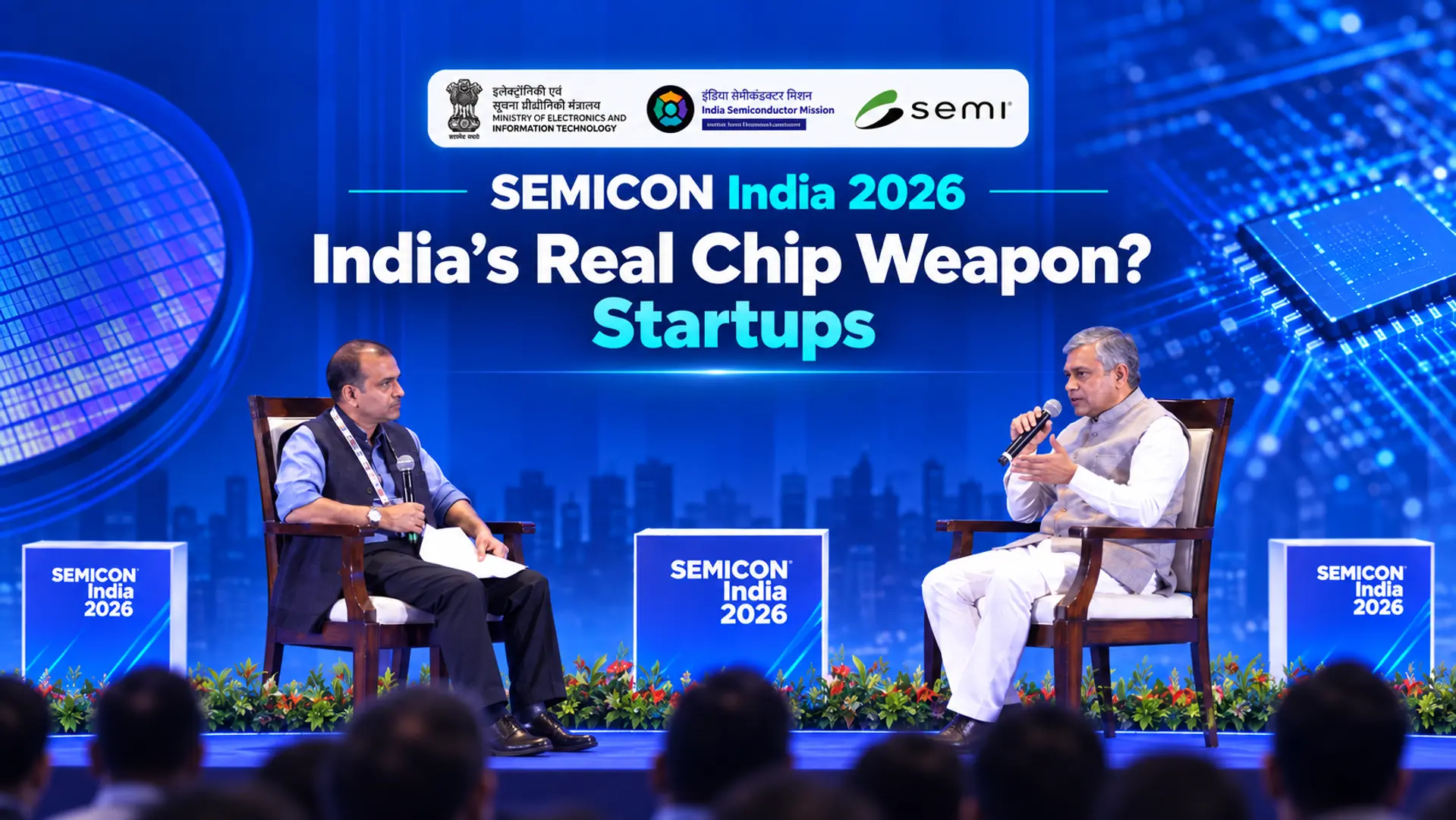

India's chip design startups are set for a significant leg up as the Union government firms up Semicon 2.0, with plans to more than double state-backed support for the segment. Union Minister for Electronics and Information Technology Ashwini Vaishnaw said as much at a fireside chat during SEMICON India 2026, held on 18 September 2026. His remarks, delivered as India's second phase of semiconductor incentives takes shape, put deep-tech chip designers and the country's MSME manufacturing base at the centre of the country's chip ambitions, alongside the marquee investments going into fabrication plants.
India's semiconductor push began under Semicon 1.0 six years ago, at a point when earlier attempts spanning nearly six decades had repeatedly faltered, largely due to inconsistent policy and short-term thinking, Vaishnaw said. This time, the government built the programme around a 20-year roadmap and a phased approach, starting with assembly, testing, marking and packaging (ATMP) units and a first fabrication plant in a high-volume, relatively less complex chip segment, the 28 nanometre to 90 nanometre node, which the minister said accounts for close to 70% of global chip volumes. Semicon 1.0 was planned as a six-year programme but was completed in four, he noted, setting up its successor.
Semicon 2.0, approved with an outlay of Rs 1,27,500 crore, rests on six pillars, design, materials and machines, additional fabs, more ATMP capacity, research and development, and talent, Vaishnaw said. Chip design has been the most startup-heavy of these so far. Under Semicon 1.0, the government tackled what Vaishnaw called the biggest barrier for young design companies: the high cost of licensing electronic design automation (EDA) tools from vendors such as Cadence, Synopsys and Siemens. Instead of funding individual licences, it routed shared access to these tools through the Centre for Development of Advanced Computing. More than 105 startups went on to become chip designers as a result, and 20 of them raised venture capital funding, reportedly worth close to Rs 800 crore, according to earlier government disclosures. Building on that base, Vaishnaw said Semicon 2.0 is targeting at least 200 deep-tech chip design companies, a scale he described as a potential game changer for India's intellectual property base.
MSMEs anchor the precision manufacturing ecosystem
Beyond chip design, Vaishnaw pointed to the effect on India's small and medium manufacturers. Citing an industry executive he had met at the event, without naming the company, he said it had already begun exporting components worth around Rs 2,000 crore from India, with close to 90% of that component ecosystem sourced from MSMEs. The precision manufacturing capabilities built up around electronics assembly, he said, are now feeding multiple sectors, including mobile phone manufacturing, aerospace components for companies such as Airbus, and defence, in addition to semiconductors. One chief executive he had spoken with, Vaishnaw added, said his company's board had told him there was effectively no cap on investment for India, as long as execution kept pace, a sign, he said, of investor confidence in the programme.
To support this shift, the government is rolling out a multi-level skilling framework, starting with a 240-hour Level 1 course meant to take a student straight out of high school toward capabilities comparable to an engineering graduate over successive levels. A dedicated Precision Manufacturing Institute is set to launch soon, to be followed by more such institutes. On the broader talent count, Vaishnaw said India had set out to train 85,000 semiconductor design engineers over ten years and had trained around 70,000 within the first four years, a figure cited in this conversation; other recent government statements have put the cumulative total at the full 85,000 target, so the precise current count appears to vary by when it was last updated. Separately, the clean room technician target of one lakh under Semicon 2.0 will likely need to be revised upward given industry demand, he said.
Why access to design software mattered more than money for chip startups
One detail from the conversation helps explain why India's chip design startup count grew as quickly as it did. EDA tools are specialised software used to lay out and simulate a chip before it goes into manufacturing, and licences from vendors such as Cadence and Synopsys can cost more than an early-stage startup's entire budget for a year. Rather than subsidising individual purchases, the government treated EDA access as shared infrastructure through C-DAC, letting startups design chips without absorbing that cost individually.
That design choice, Vaishnaw suggested, did more to seed India's chip design ecosystem than direct grants might have, since it lowered the barrier to simply attempting a chip design in the first place. Whether that model holds up for a cohort nearly twice the size under Semicon 2.0 remains one of the open questions for the next phase.
With India's first fabrication plant, the Tata Electronics-PSMC facility at Dholera, on track for its first wafer in 2028, Vaishnaw said the space reserved for that wafer in his office currently sits empty, a reminder of how much of Semicon 2.0's promise is still ahead rather than delivered. For chip design startups and the MSMEs feeding into the ecosystem, the coming phase will test whether policy support built on shared infrastructure and phased skilling can scale well beyond its founding cohort.