



From sand to the chip in your phone: India's semiconductor chief explains every step
From sand to wafer, EDA tools to dicing, test and packaging, Amitesh Kumar Sinha walks through how a chip is designed, built and finished, and what each stage costs

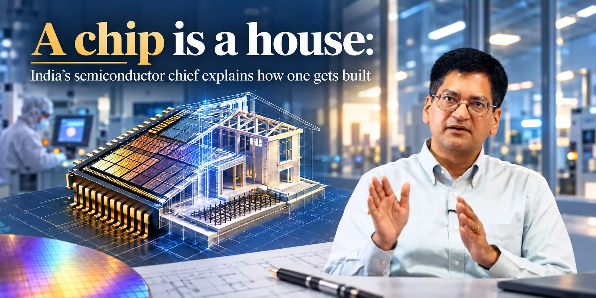

Every Indian who uses a phone, a laptop or a UPI app depends on semiconductors, and most have never seen one. As Semicon India 2026 opens in New Delhi on 17 September 2026, Amitesh Kumar Sinha, Additional Secretary at MeitY and CEO of the India Semiconductor Mission, sat down with Shradha Sharma, Founder and CEO of YourStory and The Bharat Project, and explained how a semiconductor chip is made using an analogy anyone can follow: a chip is a house.
"A house is first designed, then constructed, then finished with doors and windows so it becomes functional," Sinha said. "A chip is the same."
The explanation matters because the numbers behind it are why the government has committed Rs 1,27,500 crore to the second phase of the mission, notified on 31 August 2026.
Designing the house
Anything that carries electricity and interacts with you logically, from a search typed into Google to AI servers, defence equipment and consumer durables, runs on chips. Like a house with several floors, a chip is built in layers. A house is designed with CAD tools; a chip is designed with EDA, or electronic design automation, tools, and the design is complex enough that Sinha counts it among the most complex technologies in the world.
Design is also where most of the money is. Roughly half the value of the semiconductor chain sits in design, and a single chip design can cost anywhere from Rs 25 crore to Rs 35 crore at the simple end to Rs 1,000 crore, Rs 1,500 crore or Rs 2,000 crore for the most complex parts. That is why the mission's first phase gave startups free access to EDA tools and why the second phase adds government co-investment once a venture capital firm backs a design startup.
Building it: the foundry as kitchen
Once the design is finished on computers, it goes to a fabrication plant, or fab. The fab's engineers need the design in their own machine language, so the design team works from the foundry's process design kit, or PDK, which Sinha describes as the foundry's own EDA toolkit. The two are matched, a design file is created and transferred, and the foundry takes over. "The foundry is like a kitchen," he said. "Give it the recipe and it delivers the product."
Chips are not made one at a time. They are fabricated on a large circular wafer, which Sinha compares to the raw structure of a building: columns, pillars and walls, before the finishing. Wafers come in 12-inch, 8-inch, 6-inch and 4-inch sizes. For silicon logic and memory fabs, 12-inch is the standard; compound semiconductors such as silicon carbide and gallium nitride are usually made on 8-inch and 6-inch wafers today.
The raw ingredient is the wafer itself. Silicon is refined from quartz sand into ultra-pure crystal, grown into a cylindrical ingot and sliced into thin discs, which arrive at the fab polished to a mirror finish. Inside the fab, the recipe runs to several hundred steps: layers of material are deposited on the wafer, patterns are printed onto them with light in a process called lithography, and unwanted material is etched away, repeated layer by layer over weeks until the circuit is complete.
How many chips come out of one wafer
Think of many houses on one plot. A single wafer carries many identical chips, and a process called dicing cuts them apart. Depending on chip size, one wafer can yield anywhere from 5,000 to 50,000 chips, Sinha said.
Each diced chip, or die, then goes for packaging, which is the equivalent of adding electricity, water, doors and windows. The die is encapsulated in a plastic mould from above and below, and connectors are brought out so it can link electrically with neighbouring chips or a larger system. Only now is it functional. Chips are tested twice along the way, once on the wafer to weed out faulty dies before dicing, and again after packaging, before they ship. The packaged chips are mounted on a printed circuit board or another substrate, and many chips together form a system. A mobile phone can carry 200 to 250 chips, with separate ones for power, communication, processing and every other function.
India's first phase reflects this sequence. Of the 12 approved projects, nine are what the government calls ATMP units, for assembly, testing, marking and packaging, which cover the back end of the process from dicing to test. Packaging is where Sinha expects India to become a large exporter within five to six years. Fabs, which sit further up the chain, take longer.
Why a chip fab needs the government
Sinha's second lesson is about cost. Manufacturing a chip plant runs from around Rs 500 crore for a small facility to Rs 80,000 crore or Rs 90,000 crore for a large one, and a cutting-edge fab at the 3 nanometre or 2 nanometre node, the node being the industry's shorthand for how small and densely packed a chip's transistors are, costs 15 to 25 billion dollars, roughly the size of India's entire Semicon 2.0 outlay or more. Equipment alone is around 65% of the cost of a plant, Sinha said, followed by the chemicals, gases and materials it consumes, and then logistics, cleanroom design and manpower skilled in precision engineering, which is why Semicon 2.0 is trying to bring those suppliers to India rather than only the plants. Nowhere in the world, he said, has a semiconductor industry been built without state support. In the United States it began with defence-funded research that spilled into Silicon Valley; Japan and Taiwan followed similar paths; and countries with mature industries still offer incentives today.
The strategic argument follows from the cost. Since COVID, Sinha said, countries have turned conservative on exports and imports. A country denied access to critical chips, especially the AI compute chips young developers build on, sees its progress stall. No country controls 100% of its supply, not even the United States, but India wants enough capability that it cannot be cut off.
Visitors to Semicon India 2026 this week can see each of those stages, design, fabrication, testing and packaging, on the exhibition floor, which is the closest most people will get to watching a house of a few billion transistors go up.